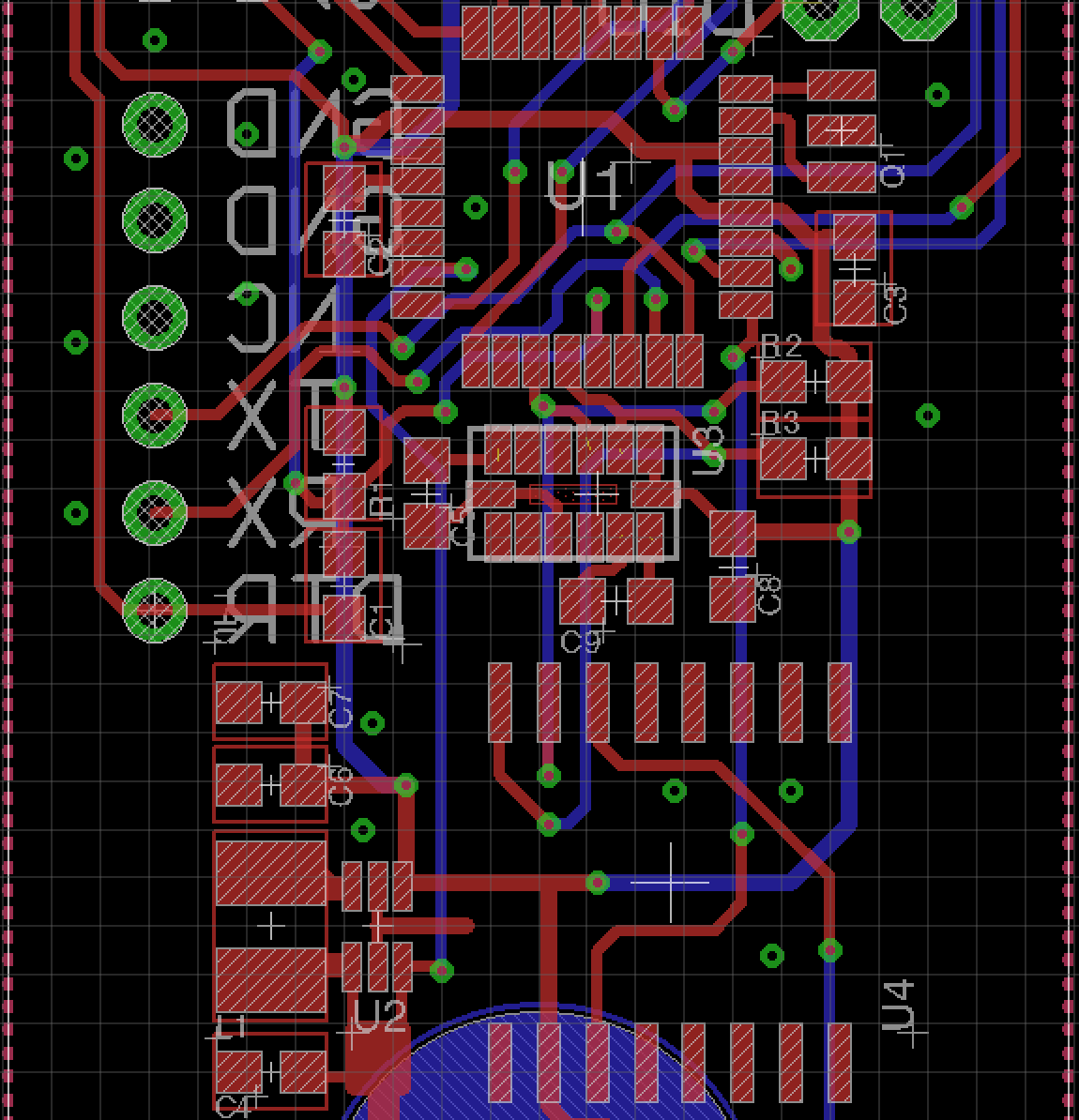
2 Layer Pcb Design
Layer layers hackaday pcbs two stackup stack laser example stuck designing try give four osh park data Double layer pcb design in ganapathi, coimbatore Pcb layer diy projects pyroelectro tutorials boards finished
What Factors Determining PCB Layers - RAYPCB
Double layer pcb Printed multilayer circuits saad hasan syed Pcb multilayer pcba flowchart routing electronicsandyou
Pcb layer board circuit electronic singapore
Multilayer pcb2 layer pcb 10cm x 15cm max australia Distinguished way of 4 layer pcb and 6 layer pcbRaspberry pi cm4 i/o board 2-layer pcb design.
Pcb layerDouble layer pcb Pcb layer 10cm 15cm max australia2 layer pcb design singapore.
![Multilayer PCB | Types of PCB | Design, Tutorial, Manufacturing Process](https://i2.wp.com/www.electronicsandyou.com/blog/wp-content/uploads/2019/03/multilayer-pcb.jpg)
Pcb stackup
What is 2 layer pcb? everything you need to know about pcbsPcb via multilayer layer multi board pcbs structure altium designing stackup process layers india manufacturing single considerations important while vias Stuck designing two-layer pcbs? give four layers a try!Pcb cm4 routing.
First 2 layer pcb design questions : askelectronicsPcb design: diy 2 layer boards Pcb designPcb layer layout designing tasarımı.
![What Factors Determining PCB Layers - RAYPCB](https://i2.wp.com/www.raypcb.com/wp-content/uploads/2021/03/b004cd776856494-1.jpg)
Pcb stack layer standard ups multi layers
Multilayer pcb manufacturing process & design guidelinesPcb layer layers allpcb distinguish tanna karan vias What factors determining pcb layersPcb layer rogers.
Two layer pcb design company rogers 4003c rogers 5880 pcb boardPcb layer stackup multilayer Pcb move layer board time layersPcb layers board circuit printed layer dielectric single factors determining conductive.
![Double Layer PCB | Construction And Applications](https://i2.wp.com/www.circuits-diy.com/wp-content/uploads/2021/01/double-layer-pcb-768x432.jpg)
Standard multi-layer pcb stack-ups 2 4 6 8 and 10 layers
.
.
![Multilayer PCB Manufacturing Process & Design Guidelines - PCB Power](https://i2.wp.com/www.pcbpower.com/content/images/Picture1(7).png)
![Stuck Designing Two-Layer PCBs? Give Four Layers A Try! | Hackaday](https://i2.wp.com/hackaday.com/wp-content/uploads/2019/03/4-layer-stackup-thumbnail.png)
![Double Layer PCB | Construction And Applications](https://i2.wp.com/i.stack.imgur.com/15la5.png)
![Double Layer PCB Design in Ganapathi, Coimbatore | ID: 17793398788](https://i2.wp.com/5.imimg.com/data5/BV/XF/MY-43956467/double-layer-pcb-design.jpg)
![PCB Stackup - BitWeenie | BitWeenie](https://i2.wp.com/www.bitweenie.com/wp-content/uploads/2013/02/LayerStackup.png)
![First 2 Layer PCB Design Questions : AskElectronics](https://i2.wp.com/external-preview.redd.it/n_HlQyhO6_buLxlQ-ODV2NAkWykXY_M9hvyV57_vozU.jpg?auto=webp&s=3ce8c78033ede5416d87bf12b72acf6d6399699a)
![pcb design - Is it time to move from a 2 layer board to a 4 layer board](https://i2.wp.com/i.stack.imgur.com/WAJwK.png)
![PCB Design: DIY 2 Layer Boards - Introduction | PyroElectro - News](https://i2.wp.com/www.pyroelectro.com/tutorials/pcb_design_diy_2_layer/img/2_layer_pcb_done.jpg)
![Raspberry Pi CM4 I/O board 2-layer PCB design - Electrical Engineering](https://i2.wp.com/i.stack.imgur.com/w3IT0.png)